


Description
Overview
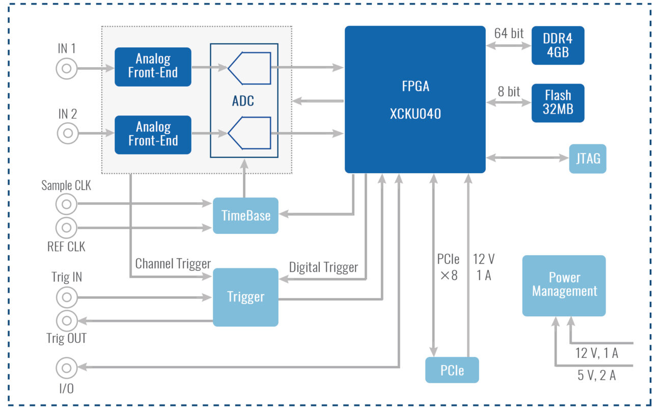
The SG1227 PCIe High-speed Acquisition Card is an 8-bit dual-channel digitizer with a maximum sampling rate of up to 5 GS/s and an analog bandwidth of up to 500 MHz. The main control chip of the Acquisition Card uses the FPGA device XCKU040 based on the Xilinx Kintex UltraScale series, which enables customized real-time processing algorithms. There is large-capacity DDR4 memory on board for long-term data acquisition. It adopts PCIe 3.0 x 8 interface, has a very high data transfer rate, occupies only one PCIe slot in the host PC, and enables high performance in a small size, which makes it an ideal platform for businesses and industries, and capable of providing customized services for hardware, FPGA, and software.
Product Block Diagram
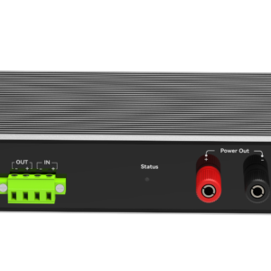
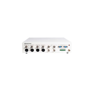
Product Show
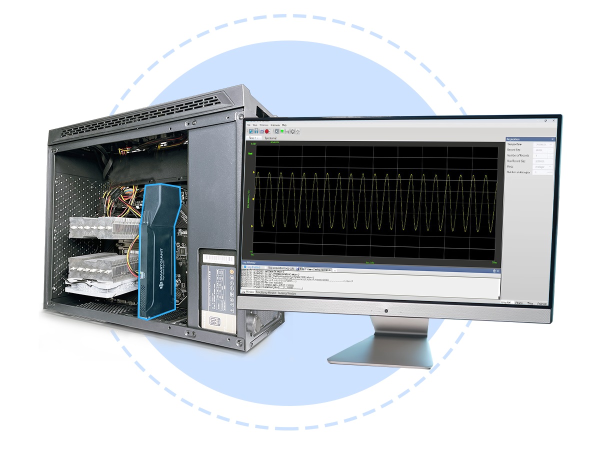
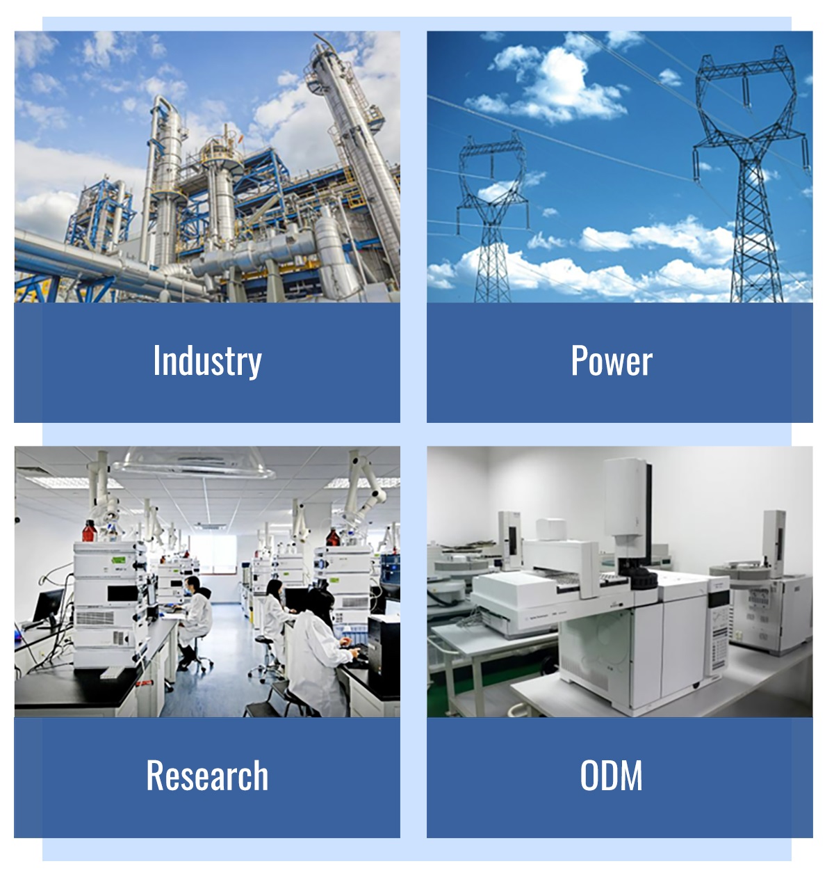
Application Scenario
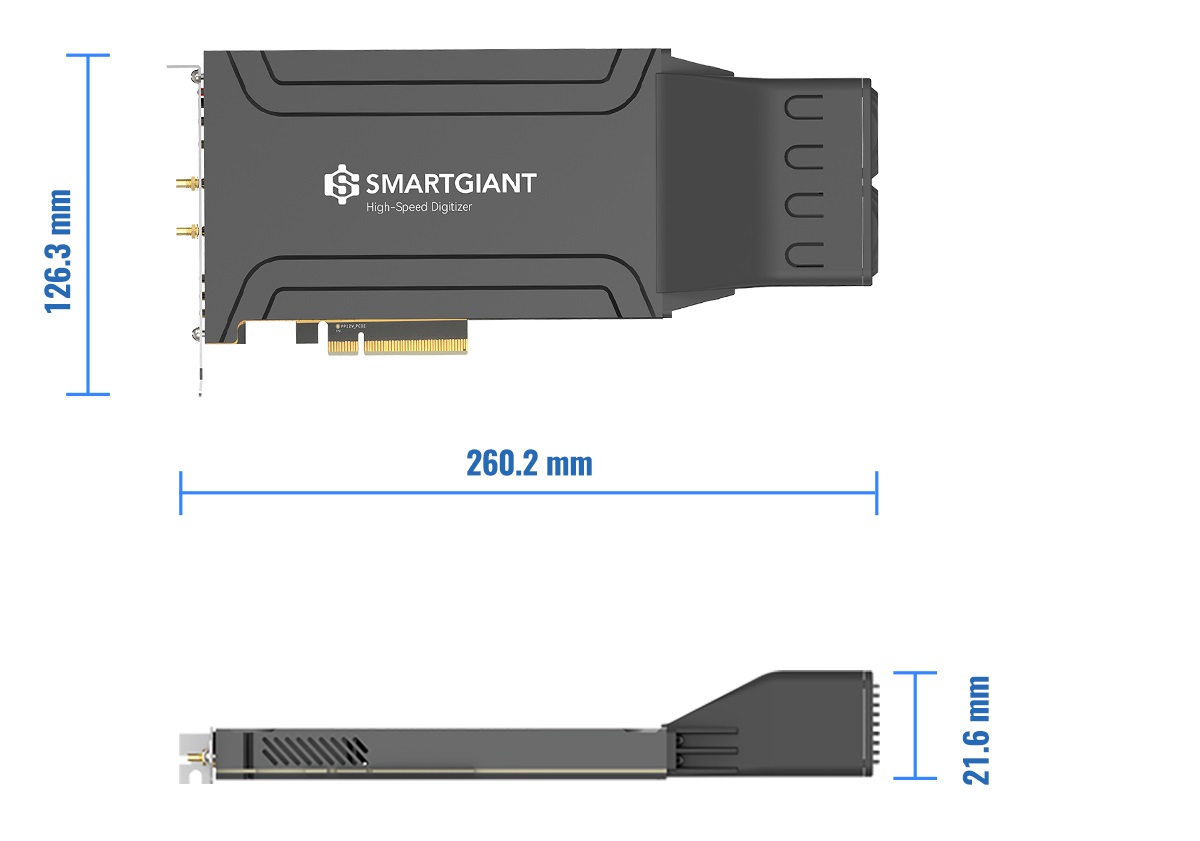
Product Size
Specification
| No. | Description | Index | ||||
| Analog Input
(IN1&IN2) |
1 | Number of Channels | 2 | |||
| 2 | Impedance | 50Ω ± 3% | ||||
| 3 | Coupling Method | DC | ||||
| 4 | Full Scale Range (FSR) | 50mV, 100mV, 200mV, 250mV, 500mV, 1V, 2V, 2.5V, 5V | ||||
| 5 | Maximum Input Voltage | 士5V DC | ||||
| 6 | Input Voltage Offset | 士 0.5 FSR | ||||
| 7 | Analog Input Bandwidth | 500 MHz | ||||
| 8 | Effective Number of Bits (ENOB) | 6.2 @10 MHz | ||||
| 9 | Signal-to-Noise Ratio (SNR) | 39 dB @ 10 MHz | ||||
| 10 | Spurious Free Dynamic Range (SFDR) | 46.5 dB @10 MHz | ||||
| 11 | Total Harmonic Distortion (THD) | -45.9 dB @10 MHz | ||||
| Digital Conversion | 12 | Resolution | 8 bits | |||
| 13 | RAM | 4 GB DDR4 and 32 MB Flash | ||||
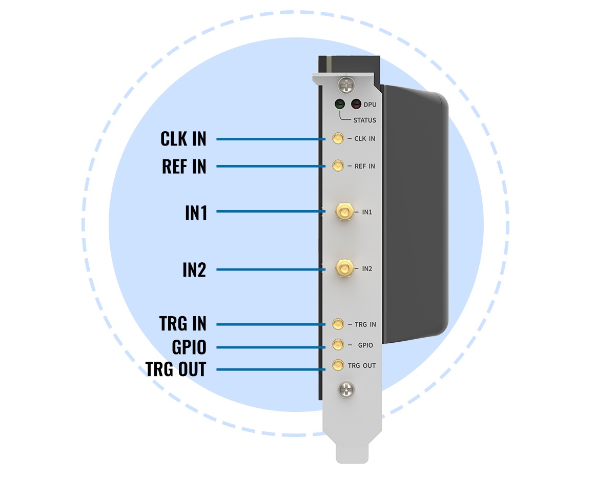
| 14 | Sampling Clock Source | Internal or external | ||||
| 15 | External Clock Source (CLKIN) | Frequency | 2.5 GHz | |||
| Level | +10 dBm to +15 dBm | |||||
| Impedance | 50Ω | |||||
| 16 | External Reference Clock Source (REF IN) | Frequency | 100 MHz | |||
| Level | -4 dBm to +6 dBm | |||||
| Impedance | 50Ω | |||||
| 17 | Maximum Number of Recording Points | 2 million | ||||
| Trigger | 18 | Trigger Mode | Rising edge/falling edge/level | |||
| 19 | Trigger Source | External, channel, software | ||||
| 20 | External Trigger (TRG IN) | Coupling Method | DC | |||
| Impedance | 50Ω | |||||
| Level Range | 士5V | |||||
| Minimum Amplitude | 0.5 Vpp | |||||
| Frequency Range | DC to 500 MHz | |||||
| 21 | Trigger Output (TRG OUT) | Quantity | 1, 500 source impedance | |||
| Signal Level | 1.8 Vpp + 2.5 V offset | |||||
| 22 | Control (GPIO) | I programmable output control IO | ||||
| Other | 23 | Communication Interface | PCle x 8 Gen3 | |||
| 24 | Operating Temperature | 0 to +50°C | ||||
| 25 | Storage Temperature | -40 to+70°C | ||||
| 26 | Power Consumption | +12 V PCle | 1A | |||
| +12V | 1.1A | |||||
| +5V | 1.4A | |||||
| 27 | Shape | Standard PCle x8 (full length w/ fan) | ||||
| 28 | Size | 260.2 x126.3x 21.6 mm | ||||
| 29 | Weight | 454g | ||||