
Description
The SG2625 FPGA Module is an SOM (System on Module) board based on Xilinx XC7Z020/010/007S All Programmable System-on-Chip (SoC) which is among the Xilinx ZYNQ-7000 family, featuring integrated dual-core ARM Cortex-A9 processor with Xilinx 7-series FPGA logic. The SG2625 module has up to 1GB DDR3 SDRAM with x32 data bus width, 4GB eMMC, 16MB quad SPI Flash, a Gigabit Ethernet PHY, an USB PHY and USB to UART on board. It provides a large number of I/O signals for ARM peripherals and FPGA I/Os through two 0.8mm pitch 120-pin board-to-board connectors, which is ideal for your next embedded design. SmartGiant also provides customization services to help customers free their hardware, logic, firmware, and software tasks, as well as ODM services from R&D, validation and mass production.
 Controllers
| Controller | FPGA Model & Parameter | Basic Specification |
| SG2625-MU01PC-Zynq 7020 | Xilinx Zynq 7020, Dual-Core ARM Cortex-A9, Atrix-7 85K-Logic Cell: | 1 GB DDR3, 4 GB eMMC, 16 MB Quad SPI Flash, 1 Gb Ethernet, USB 2.0, UART: |
| SG2625-MU02PC-Zynq 7010 | Xilinx Zynq 7010, Dual-Core ARM Cortex-A9, Atrix-7,25K-Logic_Cell; | 1 GB DDR3, 4 GB eMMC, 16 MB Quad SPI Flash, 1 Gb Ethernet, USB 2.0, UART: |
| SG2625-MU03PC-Zynq 7007 | Xilinx Zynq 7007, Single-Core ARM Cortex-A9, Atrix-7,23K-Logic_Cell; | 512 MB DDR3, 4 GB eMMC, 16MB Quad SPI Flash, 1 Gb Ethernet, USB 2.0, UART: |
| Nexus-001 -2EG | Xilinx Zynq UltraScale+ZU2EG, Quad-Core ARM, 103K-Logic_Cell, | 2 GB DDR4, 16 GB eMMC, 1 Gb Ethernet, USB 3.0 Type-C, UART: |
| Nexus-002 -4EG | Xilinx Zynq UltraScale+ZU4EG, Quad-Core ARM, 192K-Logic_Cell, 16 lane Serdes; | 2 GB DDR4, 16 GB eMMC, 1 Gb Ethernet, USB 3.0 Type-C, UART: |
| Nexus-003 -7EG | Xilinx Zynq UltraScale+ZU7EG, Quad-Core ARM, 504K-Logic_Cell; | 2 GB DDR4, 16 GB eMMC, 1 Gb Ethernet, USB 3.0 Type-C, UART; |
Application Scenarios
- FPGA Controller
- Digital Signal Processing
- Algorithm Acceleration
- Emulation & Prototyping
- Data Center
- Industrial & Vision
- Healthcare & Sciences
- Test& Measurement
- Wired & Wireless Communications
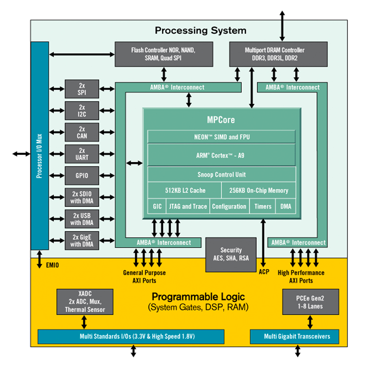
Processing System (PS)
| Core | Dual ARM® Cortex™-A9 MPCore™ with CoreSight™ |
| Clock | 866 MHz |
| L1 Cache | 32 KB Level 1 4-way set-associative instruction and data caches (independent for each CPU) |
| L2 Cache | 512 KB 8-way set-associative Level 2 cache |
| On-Chip Memory | 256 KB |
| External Memory Interfaces | DDR3, DDR3L, DDR2, LPDDR2 |
| Static Memory Interfaces | 2x Quad-SPI, NAND, NOR |
| 8-Channel DMA Controller | Memory-to-memory, memory-to-peripheral, peripheral-to-memory, and scatter-gather transaction support |
| I/O Peripherals and Interfaces | 2x UART, 2x CAN 2.0B, 2x I2C, 2x SPI, 4x 32b GPIOs, 2x USB 2.0 (OTG), 2x Tri-mode Gigabit Ethernet, 2x SD/SDIO |
Programmable Logic (PL)
| SG2625-MU01PC | SG2625-MU02PC | SG2625-MU03PC | |
| MPSoC | XC7Z020 | XC7Z010 | XC7Z007S |
| Logic Core | Xilinx 7 Series
Artix®-7 FPGA |
Xilinx 7 Series
Artix®-7 FPGA |
Xilinx 7 Series
Artix®-7 FPGA |
| Programmable Logic Cells | 85K Logic Cells | 28K Logic Cells | 23K Logic Cells |
| Look-Up Tables (LUTs) | 53,200 | 17,600 | 14,400 |
| Flip-Flops | 106,400 | 35,200 | 28,800 |
| Total Block RAM | 4.9Mb (140) | 2.1Mb (60) | 1.8Mb (50) |
| Programmable DSP Slices | 220 | 80 | 66 |
Basic Specifications
| Power Supply Voltage | DC5V; <2A |
| Power Dissipation | <10W |
| CPU Clock | Up to 866MHz |
| DDR3 Clock | 533MHz |
| RAM | Up to 1GByte |
| Flash | 16M Byte(Q-SPI),4G Byte(eMMC) |
| Ethernet | 10/100/1000M ,1 channel. |
| USB | USB 2.0 OTG, 1 channel. |
| Serial ports | 115200 bps ,1 channel. |
| Digital I/O | Bank500(ARM) 6pin(Can be configured SPI,IIC,SDIO,UART,CAN) 1.8V
Bank501(ARM) 6pin(Can be configured SPI,IIC,SDIO,UART,CAN) 3.3V Bank13 (FPGA)25pin(12 LVDS pairs and 1 single-ended I/O)Can be configured as LVCMOS18 or LVCMOS25 or LVCMOS33. Bank13 is only available in XC7Z020 (SG2625-MU01PC-F). Bank34 (FPGA)50pin(24 LVDS pairs and 2 single-ended I/O)Can be configured as LVCMOS18 or LVCMOS25 or LVCMOS33 Bank35 (FPGA) 49Pin(24 LVDS pairs and 1 single-ended I/O)Can be configured as LVCMOS18 or LVCMOS25 or LVCMOS33 |
| Clock Source Stability | ±10 ppm @-40 ~ +105°C |
| Interface | Two 120pin board-to-board connectors |
| Operating Environment | 0 to 50°C / 0 % to 80 % R.H. |
| Storage Environment | -40 to 70°C / 0 % to 80 % R.H. |
| Dimensions | 75mm×55mm |
| Thickness | 1.6mm |
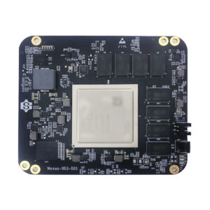
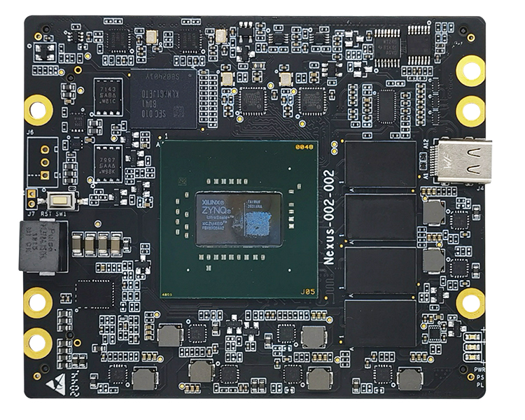
Module Appearance
Function Block Diagram
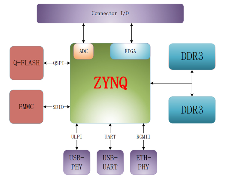
Zynq7020 FPGA Block Diagram SOC (ARM+FPGA) Architecture
The ZYNQ®-7000 family is based on the Xilinx All Programmable SoC architecture. These products integrate a feature-rich dual-core ARM® Cortex™-A9 based processing system (PS) and 28 nm Xilinx programmable logic (PL) in a single device. The ARM Cortex-A9 CPUs are the heart of the PS and also include on-chip memory, external memory interfaces, and a rich set of peripheral connectivity interfaces. These devices combine the software programmability of a Processor with the hardware programmability of an FPGA, resulting in unrivaled levels of system performance, flexibility, scalability while providing system benefits in terms of power reduction, lower cost with fast time to market. Unlike traditional SOC processing solutions, the flexible programmable logic of the ZYNQ-7000 devices enables optimization and differentiation, allowing designers to add peripherals and accelerators to adapt to a broad base of applications.